Slow wire walking, also called low-speed wire walking, is a kind of CNC machining machine tool that uses continuously moving fine metal wire as an electrode to pulse spark discharge on the workpiece to generate a high temperature of over 6000 degrees, ablate metal and cut into a workpiece. The principle of wire processing is the phenomenon that there is a gap between the wire electrode and the workpiece, and the metal is removed by continuous discharge. Since the slow-moving wire cutting machine adopts the method of wire electrode continuous feeding, that is, the wire electrode is processed during the movement, so even if the wire electrode is worn out, it can be continuously supplemented, so it can improve the machining accuracy of the parts and slow the wire. The surface roughness of the workpiece processed by the cutting machine can usually reach Ra=0.8μm and above, and the roundness error, linear error and dimensional error of the slow-moving wire cutting machine are much bett...
CNC machining and numerical control machining are a method to control the movement of machine tools and the production process of machining through computer digitization and information digitization. It is an intelligent numerical control device developed as an economical, high-speed, reliable, multi-functional, intelligent, and open structure. CNC machining is also an important indicator that can measure the continuous level and comprehensive ability of a safety technology, as well as the degree of modernization of related science and technology capabilities, especially in aviation, biology, medical and other high-tech cultural industries, and it is also a powerful indicator. reflect. So, what errors may occur during CNC machining and CNC machining? Let us understand together: The use of approximate machining motion or approximate tool contours causes errors in the CNC principle of machining. The reason why it is called machining principle error is because of the error in machi...
The Purpose Standardize the management of the scrapping of the company's metal stamping dies, prevent the loss of company assets, and formulate this system specially. Scope of application It is suitable for the management of the company's scrap molds. Definition If the molds listed in the assets of the company fall under one of the following circumstances, the use management department may apply for scrapping. 1. Molds that exceed the specified service life. 2. The mold is severely damaged by accidents or accidents, and molds that cannot be repaired or have no repair value. 3. Metal stamping dies that have not reached the service life, but due to safety, quality, efficiency and other issues, the repair still fails to meet the minimum requirements of the customer's product process or affects the production safety and efficiency. 4. Product customers have stopped placing orders or have not placed orders for molds in several years. 4. Responsibilities 1. Responsibilities of th...
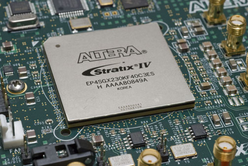
FPGA design is not a simple chip research, but mainly uses the FPGA model to design products in other industries. Unlike ASICs, FPGAs are widely used in the communications industry. Through the analysis of the global FPGA product market and related suppliers, combined with the current actual situation in my country and domestic leading FPGA products, we can discover the future development direction of related technologies, which will play a very important role in promoting the overall improvement of my country's technological level.
FPGA
Compared with traditional chip design, FPGA chips are not simply limited to research and design chips, but can be optimized for products in many fields with the help of specific chip models. From the perspective of chip devices, FPGA itself constitutes a typical integrated circuit in a semi-custom circuit, which contains a digital management module, an embedded unit, an output unit, and an input unit. On this basis, it is necessary for FPGA chips to focus on comprehensive chip optimization design, and to add new chip functions by improving the current chip design, thereby achieving the simplification and performance improvement of the overall chip structure.
Basic structure FPGA device is a kind of semi-custom circuit in the application-specific integrated circuit, which is a programmable logic array, which can effectively solve the problem of fewer gate circuits in the original device. The basic structure of FPGA includes programmable input and output units, configurable logic blocks, digital clock management modules, embedded block RAM, wiring resources, embedded dedicated hard cores, and underlying embedded functional units. Because FPGA has the characteristics of abundant wiring resources, repeatable programming, high integration, and low investment, it has been widely used in the field of digital circuit design. The FPGA design process includes algorithm design, code simulation and design, board debugging, designers and actual needs to establish the algorithm architecture, use EDA to establish a design plan or HD to write design code, through code simulation to ensure that the design plan meets actual requirements, and finally board Level debugging, use the configuration circuit to download the relevant files to the FPGA chip to verify the actual operation effect.
Working Principle FPGA adopts the concept of logic cell array LCA (Logic Cell Array), which includes three parts: Configurable Logic Block (CLB), Input Output Block (IOB) and Interconnect. Field programmable gate array (FPGA) is a programmable device. Compared with traditional logic circuits and gate arrays (such as PAL, GAL and CPLD devices), FPGA has a different structure. FPGA uses a small look-up table (16×1RAM) to realize combinational logic. Each look-up table is connected to the input of a D flip-flop, and the flip-flop drives other logic circuits or I/O to form a combination that can be realized. The logic function can also realize the basic logic unit module of the sequential logic function. These modules are connected to each other or I/O modules by metal wires. FPGA logic is realized by loading programming data into the internal static storage unit. The value stored in the memory unit determines the logic function of the logic unit and the connection between modules or between modules and I/O, and finally determines The function that FPGA can realize, FPGA allows unlimited programming.
Need an expert? you are more than welcomed to
leave your contact info and we will be in touch shortlyYOUR COMPANY
Sifangyuan Industrial Park, Xinshapu, Huaide Community
Humen town, Dongguan City, Guangdong Province. 860769-82886112 860769-82886112